
VHDL (VHSIC Hardware Description Language) is a powerful hardware description language used for describing, simulating, and synthesizing digital systems. In this article, we will explore the steps that a VHDL designer should follow. We will examine each stage, from coding and simulation to synthesis and implementation, and finally, debugging and verification.
Coding and Simulation
Basics of VHDL Coding
The VHDL coding process begins with defining the behavior or structure of digital circuits. The fundamental building blocks of VHDL include entity, architecture, and process. The entity defines the inputs and outputs of a module, while the architecture describes the relationships or behaviors between these inputs and outputs. The process structure is used to define time-dependent operations, allowing for the description of sequential logic in digital circuits.
Unwritten Rule: Only one “entity” and “architecture” should be defined within a single HDL file. Additionally, all names, including special characters, should be written in lowercase.
One of the most important aspects of coding is ensuring readability and reusability. Adopting a modular approach and coding different parts of the design as independent modules can be very beneficial. This approach makes the design easier to understand and maintain.
Unwritten Rule: Signal and variable names should be written in lowercase, while constants and generic constants should be in uppercase.
Simulation Tools and Techniques
Simulation is a critical step in testing the accuracy of the design and identifying potential errors early in the process. VHDL codes are tested using simulation tools to verify whether the design behaves as expected. Tools like ModelSim, GHDL, and Vivado are commonly used platforms by designers.
One of the most common techniques used during simulation is writing a testbench. A testbench simulates how the design will receive data from the external world and how it will process that data. All scenarios of the design should be testable, and the simulation results should be carefully analyzed. At this stage, timing diagrams of the design are examined, and the accuracy of the expected outputs is checked.
Unwritten Rule: The names of signals should be meaningful, reflecting the function of the block or signal.
Synthesis and Implementation
Synthesis Process and Tools
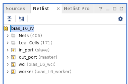
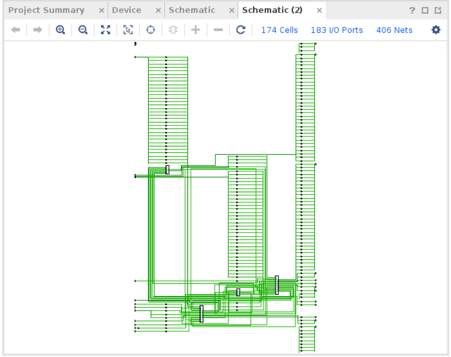
Synthesis is the step where VHDL code is transformed into a hardware structure. In this process, the design is converted into a physical circuit using logic gates, flip-flops, and other basic components. Synthesis tools optimize the design to ensure efficient use of hardware resources.
Tools like Xilinx Vivado and Altera Quartus are commonly used for FPGA (Field Programmable Gate Array) designs, while Cadence and Synopsys are preferred for ASIC (Application-Specific Integrated Circuit) designs. These tools automate all the necessary steps to convert the code into a physical circuit and significantly speed up the synthesis process.
Unwritten Rule: Avoid coding that synthesizes latches in designs. Latches can cause timing problems.
Using VHDL in FPGAs and ASICs
FPGAs offer significant advantages in the design process due to their programmability and rapid prototyping capabilities. VHDL designs on FPGAs can be quickly tested and easily modified when necessary. In ASICs, however, the design must be meticulously verified to ensure correctness before moving to production. ASIC designs typically involve a costly and lengthy production process, so the margin for error is very low.
Debugging and Verification
Debugging is one of the most critical stages in the digital design process. In this stage, all tests and analyses are conducted to prevent the design from behaving unexpectedly or undesirably and to ensure that it functions correctly. Common errors in VHDL designs include timing problems, synchronization errors, and logical errors. Identifying and correcting these errors enhances the reliability of the design.
Debugging Techniques
Some important techniques and terms used during debugging include:
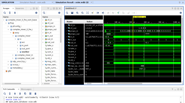
- Waveform Analysis: Waveform analysis involves examining the signal waveforms generated during VHDL simulation. This technique visualizes how the design behaves over specific time intervals. The waveform provides a graphical representation of signal values over time. This allows designers to check if a particular signal takes the correct value at the expected time.
- Timestep: Timestep allows the simulation to proceed step by step. In each step, changes in the signals and operations within the design are observed. This method is especially useful for identifying complex timing errors. Timestep enables a much more detailed analysis of how the design behaves over a specific time period.
- Assertion: Assertion statements automatically check whether certain conditions in the design are met. These statements verify that the design operates correctly and can generate error reports if unexpected situations arise. Assertion statements are typically defined in the code using the “assert” command and produce an error message during simulation if a specified condition is not met.
- Case Statements: Case statements allow a signal to exhibit different behaviors for various conditions. However, the “when OTHERS =>” clause must always be defined in these statements. This clause enables the design to behave in a specific way when the case structure encounters an undefined condition, preventing potential errors.
- Debugging Tools: Many tools are available to facilitate the debugging process in VHDL designs. ModelSim, Vivado, GHDL, and other simulation tools provide designers with the ability to detect and resolve errors. These tools help identify the part of the design where a problem occurs by monitoring error messages and warnings during simulation.
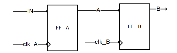
- Synchronization Errors: Synchronization errors occur when signals operating in different clock domains fail to work harmoniously together. These errors can arise especially in Clock Domain Crossing (CDC) structures. To prevent synchronization errors, signals should be properly registered, and timing checks should be carefully performed.
Testbench Writing and Verification Processes
A testbench is a structure used to verify that the design functions correctly. The testbench applies various data sets to the design’s inputs and checks whether the outputs produce the expected values. A properly written testbench should be able to test all possible conditions of the design and identify any error conditions.
Important Considerations When Writing a Testbench:
- Comprehensive Test Scenarios: The testbench should be written to cover every condition of the design. For example, all possible input combinations and edge cases should be tested.
- Verification Conditions: Assertion statements used within the testbench should ensure that the design meets all specified requirements.
- Timing Control: Waveform and timestep features provided by simulation tools should be used to detect timing issues.
Unwritten Rule: When using structures like RAM and FIFO in designs, IPs provided by FPGA manufacturers should be used, and these structures should be optimized according to the design.
This article was first published on LinkedIn on 13 August 2024.