What is FPGA?
FPGA, or Field Programmable Gate Array, is one of the most flexible and powerful tools in the world of electronics. FPGA is a hardware platform capable of implementing various digital circuits through its programmable logic gates. These devices allow a hardware designer to reconfigure their circuits, making FPGAs suitable for a wide range of applications.
Importance and Applications of FPGA
The importance of FPGAs stems from their flexibility and performance. Here are some key application areas:
- Digital Signal Processing (DSP): FPGAs can quickly process audio and video signals, making them ideal for high-resolution video and advanced audio processing applications.
- Embedded Systems: FPGAs can work alongside microcontrollers and microprocessors to create complex embedded systems.
- Communication and Network Systems: From managing internet traffic to data centers, FPGAs are used extensively.
- Automotive and Aviation Electronics: FPGAs provide reliable and fast solutions for the control systems of vehicles and aircraft.
- Artificial Intelligence and Machine Learning: FPGAs are used in AI applications to process complex algorithms quickly.
History of FPGA
Evolution of Programmable Logic Technology
The origins of FPGAs can be traced back to the 1960s and 1970s with basic logic gates and flip-flops. During this period, engineers designed digital circuits manually, and everything was much simpler. However, these basic building blocks formed the foundation of modern FPGAs.
1960s and 1970s: Basic Logic Gates and Flip-Flops
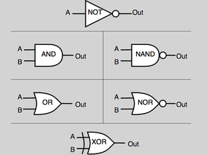
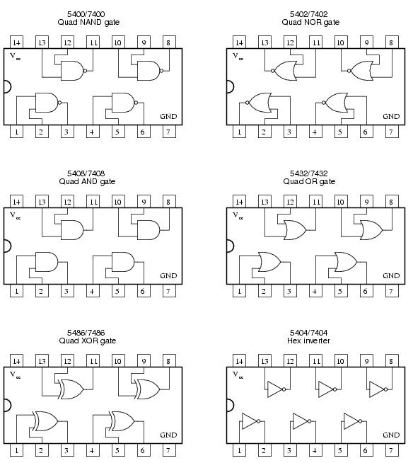
In the 1960s and 1970s, engineers used basic logic gates like NAND, NOR, AND, and OR, along with flip-flops to design digital circuits. These gates and flip-flops were the fundamental building blocks of digital electronics. Everything had to be done manually back then.
TTL Integrated Circuits
In the 1970s, Transistor-Transistor Logic (TTL) integrated circuits emerged. These circuits grouped logic gates and flip-flops into a single package, simplifying engineers’ work and allowing for more complex digital designs.
1980s: Development of PLA and PAL
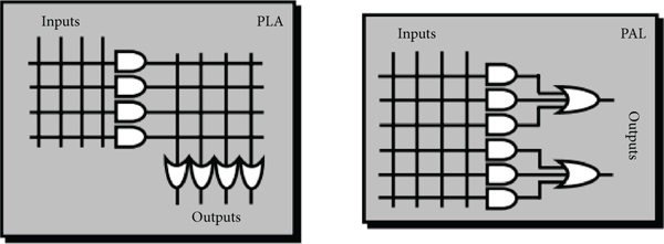
In the 1980s, Programmable Logic Arrays (PLA) and Programmable Array Logic (PAL) devices were developed. PLAs could combine basic logic gates to perform specific logic functions, while PALs included memory elements for more complex operations.
1990s and Beyond: Emergence of CPLD and FPGA
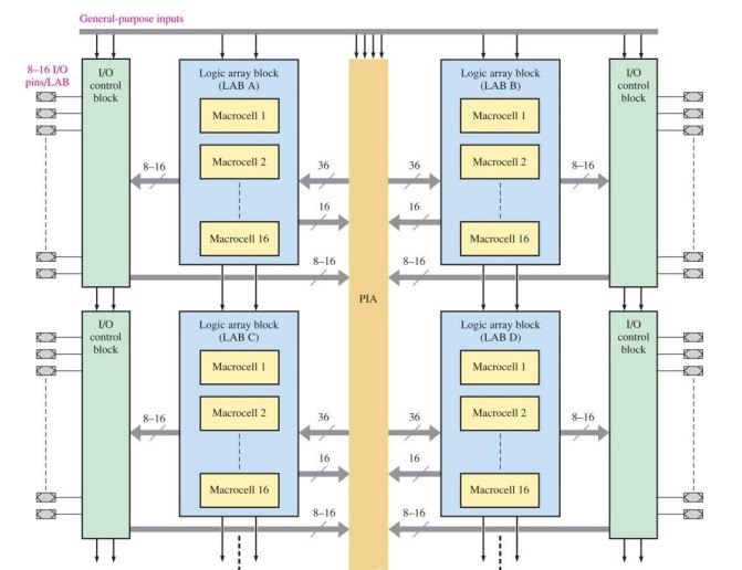
By the 1990s, Complex Programmable Logic Devices (CPLD) and FPGAs emerged. CPLDs combined multiple PAL or PLA devices into a single chip, allowing for larger and more complex designs. FPGAs, with their flexible and programmable nature, revolutionized digital design.
FPGA Architecture
Fundamental Components
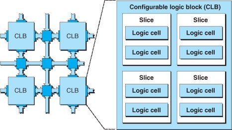
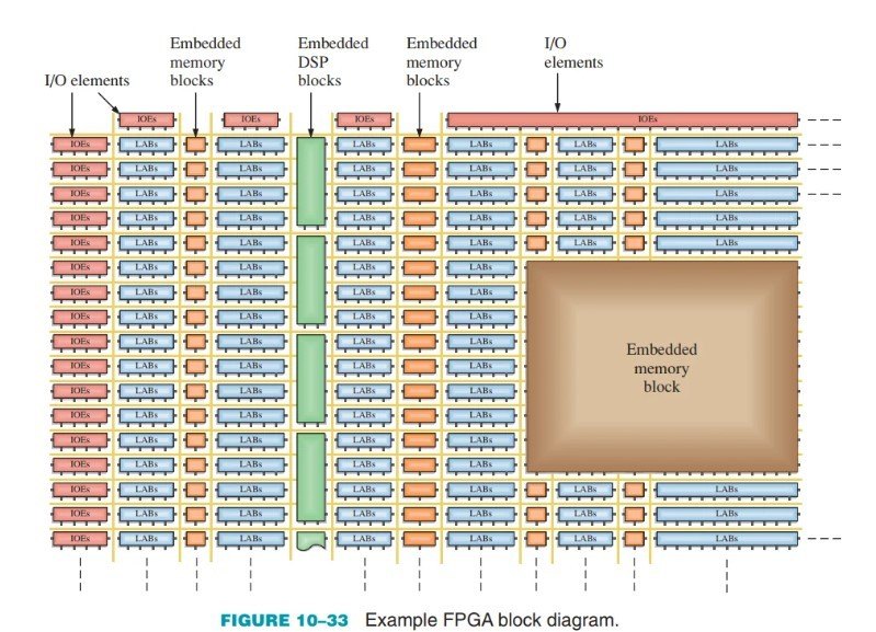
An FPGA is like a digital city. Here are some key structures and their functions:
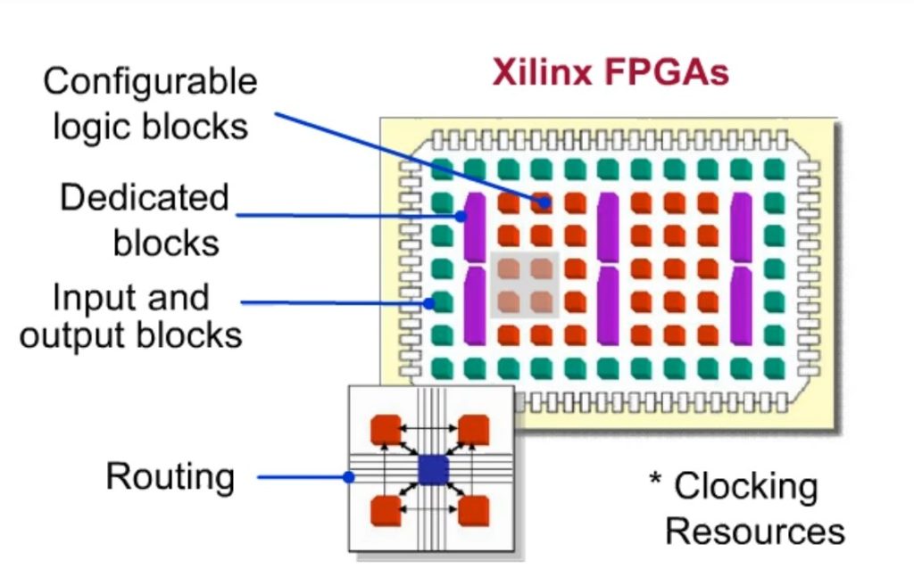
- Logic Elements (LE): The most basic building blocks of an FPGA. They can perform small logic operations and work together to form large circuits.
- Configuration Memory: Controls the programmable nature of the FPGA, determining what each logic element does.
- Input/Output Blocks (I/O Blocks): Facilitate communication between the FPGA and the outside world, managing data input and output.
- Internal Connections and Switching Matrix: Connect the logic elements within the FPGA, acting like the roads and highways of the city.
LAB (Logic Array Blocks) and CLB (Configurable Logic Blocks)
The logic elements within an FPGA are organized into groups called LABs and CLBs. These groups work together to perform larger and more complex functions.
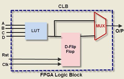
LUT (Look-Up Table) and Flip-Flops
- LUT (Look-Up Table): LUTs are the decision-making mechanism of the FPGA, storing output values for specific input combinations.
- Flip-Flops: Memory elements that store a single bit of data and are triggered by specific clock signals.
Embedded Memory and DSP Blocks
- Embedded Memory: Small, fast-access memory units within the FPGA for storing and retrieving data quickly.
- DSP Blocks (Digital Signal Processing Blocks): Special units capable of performing complex mathematical operations, used especially in audio and video processing applications.
Phase-Locked Loops (PLL) and Clock Management
- PLL (Phase-Locked Loop): PLLs regulate clock signals and synchronize different clock frequencies.
- Clock Management: Ensures that processes within the FPGA are synchronized and occur at the correct times.
FPGA Manufacturing Process
Design and Verification
This phase involves designing and verifying the FPGA’s digital structure.
- Hardware Description Language (HDL) Usage (VHDL, Verilog): HDLs like VHDL and Verilog are used to define the structure and functions of FPGAs. These languages create the logical structure of the FPGA.
- Simulation and Verification Tools (ModelSim, Vivado): Tools like ModelSim and Vivado are used to verify that the design functions correctly. These tools help detect design errors early in the process.
Synthesis and Mapping
In this phase, the HDL-defined design is translated into physical circuit elements.
- Synthesis Software and Process (Quartus II, Vivado): Synthesis translates HDL code into physical hardware components. Tools like Quartus II and Vivado manage this process, converting the design into logic gates and flip-flops.
- Post-Synthesis Optimizations: After synthesis, optimizations are performed to enhance the design’s performance, making it faster and more efficient.
Placement and Routing
This phase involves physically placing the synthesized design onto the FPGA and establishing connections.
- Physical Design and Placement: The synthesized logic elements are placed within the FPGA. This placement ensures that the circuit elements are distributed appropriately across the FPGA’s physical structure.
- Routing and Timing Analysis: Connections between the placed logic elements are established, and timing analysis ensures signals reach their destinations at the correct times.
Physical Production of FPGA
After design and verification, the FPGA is physically produced.
- Wafer Production: The foundation of FPGAs is built on silicon wafers. These wafers are made from pure silicon crystals and contain millions of transistors.
- Photolithography: Silicon wafers are processed using photolithography, a technique that uses light to draw fine patterns on the silicon. These patterns form the logic gates and connections within the FPGA.
- Ion Implantation and Diffusion: In this phase, ion implantation and diffusion techniques create transistors on the wafers, altering their electrical properties.
- Metallization and Interconnection Layers: After the transistors are created, metallization connects different circuit elements with metal layers, forming electrical connections.
- Testing and Packaging: The produced FPGAs undergo extensive testing to verify functionality. After passing tests, FPGAs are packaged appropriately for end-users.
FPGA Configuration and Programming
Configuration Memory Types (SRAM, Flash)
The configuration data for FPGAs is stored in memory types like SRAM or Flash. These memories determine the functions the FPGA will perform upon startup.
Configuration File Creation
After synthesis, placement, and routing, configuration files are created to program the FPGA. These files enable the FPGA to execute the designed functions.
Active and Passive Programming Methods
FPGAs can be programmed using active or passive methods. In active programming, the FPGA reads its configuration file and programs itself. In passive programming, an external device programs the FPGA.
JTAG and Other Programming Interfaces
FPGAs can also be programmed using interfaces like JTAG. These interfaces provide direct connections to the FPGA, facilitating programming.
Conclusion
In this article, we explored what FPGAs are, their history, architecture, and manufacturing process. FPGAs are versatile and high-performance devices used widely in the digital world. In the next section, we will compare CPLD, ASIC, and FPGA technologies, detailing the advantages and disadvantages of each. This comparison will help you choose the most suitable technology for your projects.
This article was first published on LinkedIn on 11 June 2024.